狠甩韓國三星
Taiwan Semiconductor Manufacturing Company has achieved a significant breakthrough in its research and development for the 2nm semiconductor manufacturing node.
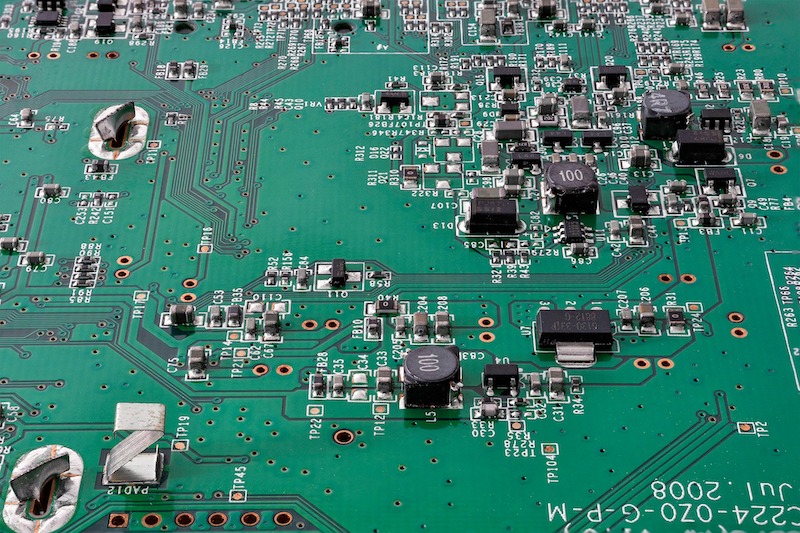
台灣積體電路製造公司(台積電)最近在2奈米半導體製程節點的研發方面取得重大突破。
research and development 研究與開發nm=nanometer奈米semiconductor(n.)半導體node(n.)節點
According to sources from its supply chain, the world’s largest contract chipmaker is expected to enter trial production of the 2nm process with a yield rate reaching 90% in the second half of 2023 and commence mass production in 2024.
供應鏈透露,業界看好台積電2023年下半年風險性試產良率即可達九成,2024年可開始量產,
contract chipmaker 代工晶片製造商trial production 試生產yield rate良率commence(v.)開始、著手=begin=startmass production大量生產mass-produce(v.)量產
This will set TSMC further apart from its rival Samsung and helps it continue to receive orders from manufacturers such as Apple and Nvidia in the future.
未來台積電將更進一步超越對手三星,助攻未來持續拿下蘋果、輝達等大廠的訂單。
set…apart from…使…與…不同;使…從…當中脫穎而出rival(n.)競爭對手=competitor
The upcoming 2nm process will adopt a new multi-bridge channel field-effect transistor architecture, as opposed to the fin-type field-effect transistor architecture used in the 3nm and 5nm processes, which has the physical limitations of current control leakage caused by process shrinkage.
有別於3奈米與5奈米採用鰭式場效電晶體(FinFET)架構,會因製程微縮產生電流控制漏電的物理極限問題,台積電2奈米改採全新的多橋通道場效電晶體(MBCFET)架構。
adopt(v.)採用;採納=employmulti-bridge channel field-effect transistor architecture多橋通道場效電晶體(MBCFET)架構fin-type field-effect transistor architecture鰭式場效電晶體(FinFET)架構as opposed to…有別於;而不是=rather thanlimitation(n.)限制、侷限current control leakage電流控制漏電shrinkage(n.)微縮、縮水、縮小
TSMC is planning to open a new cutting-edge research and development center in Hsinchu next year for the 2nm process, while seeking to acquire land next door to the new R&D center to build a production fab for 2-nano products, said the company’s senior vice president Kevin Zhang.
台積電業務開發資深副總經理張曉強指出,公司計劃在明年啟用2奈米製程研發中心,將會選擇落腳新竹,而目前興建晶圓廠的土地正在取得當中。
cutting-edge(adj.)領先的、尖端的=state-of-the-art=advancedacquire(v.)獲得;取得;購得fab(n.)(電子)晶片製造廠
TSMC’s aggressive investments in the 2nm process are a response to the rapid growth of the foundry market.
台積電因應晶圓代工市場快速成長強勢投資2奈米製程。
aggressive(adj.)積極進取的、有衝勁的、雄心勃勃的a response to~針對…的回應foundry(n.)鑄造廠、晶圓代工iron foundry鑄鐵廠glass foundry玻璃廠wafer foundry晶圓代工廠
Market research firm Omdia estimated that the global foundry market will surpass US$81 billion next year from $60.9 billion in 2017.
市場研究公司Omdia估計,全球晶圓代工市場將從2017年的609億美元增長到明年突破810億美元。
surpass(v.)超過;超越=exceed=go beyond
The company’s facility investment is expected to increase from US$14.9 billion in 2019 to US$17 billion in 2020.
台積電的投資預計將從2019年的149億美元成長至2020年的170億美元。